

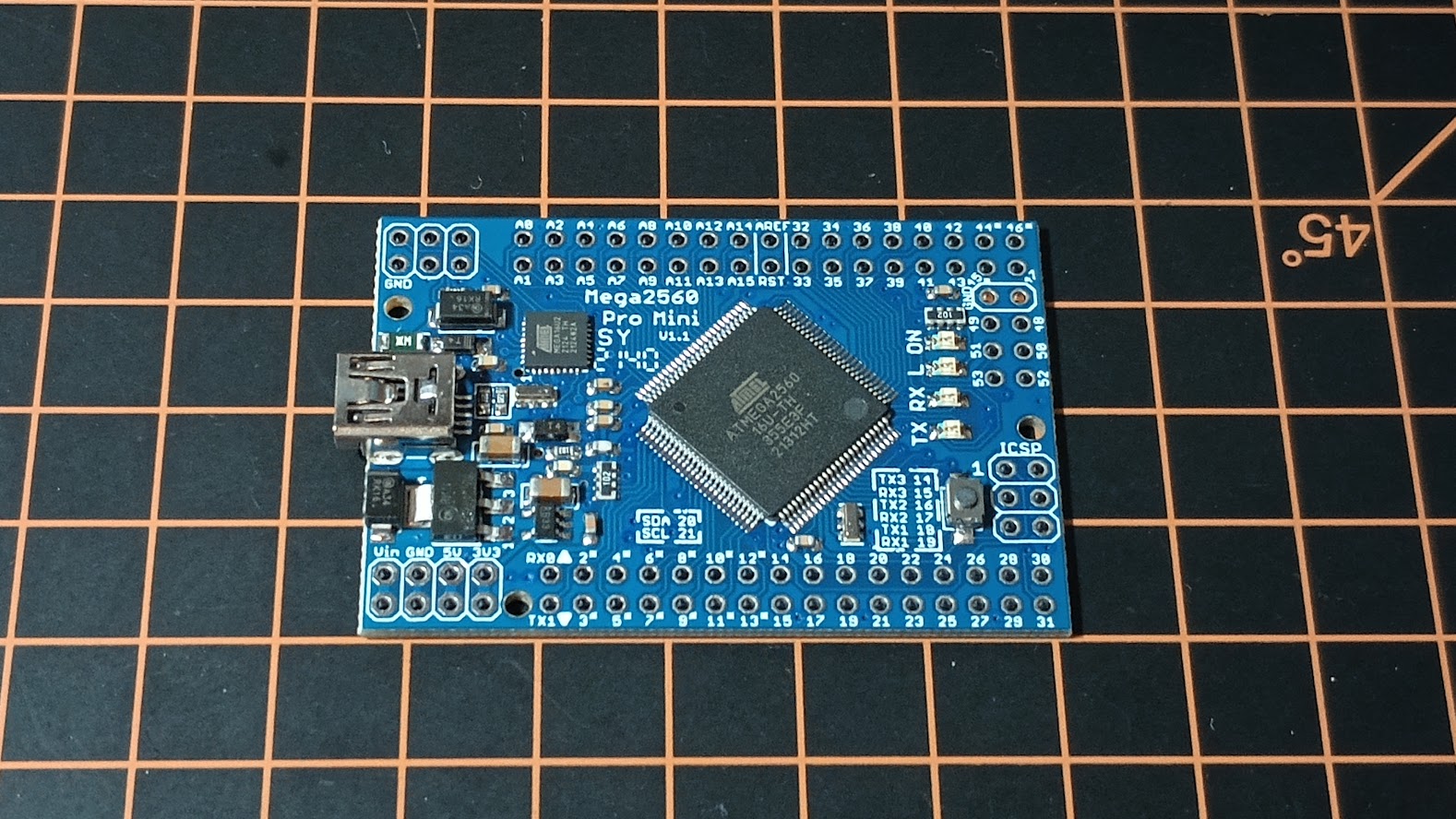
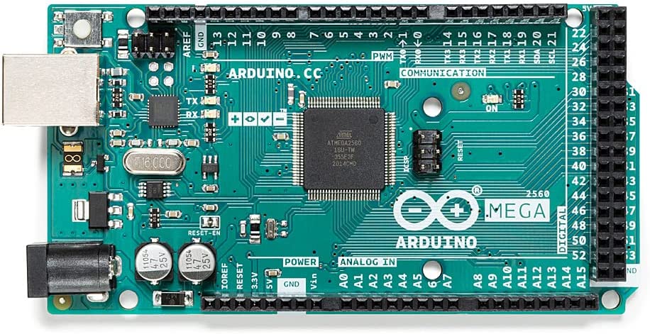
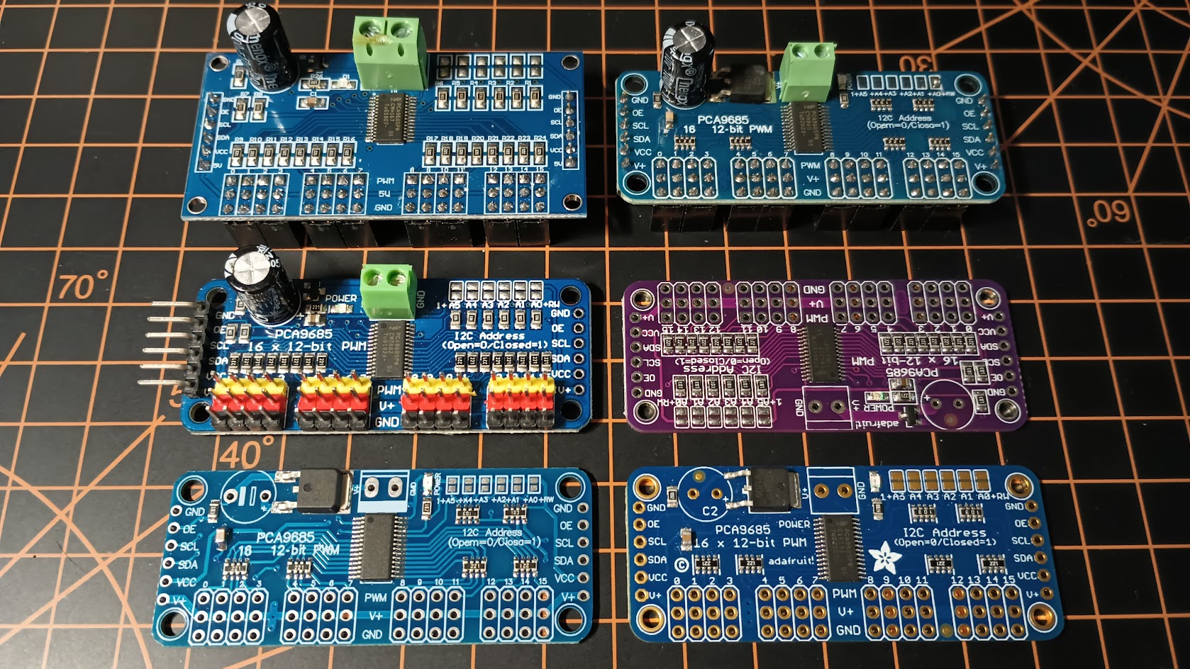
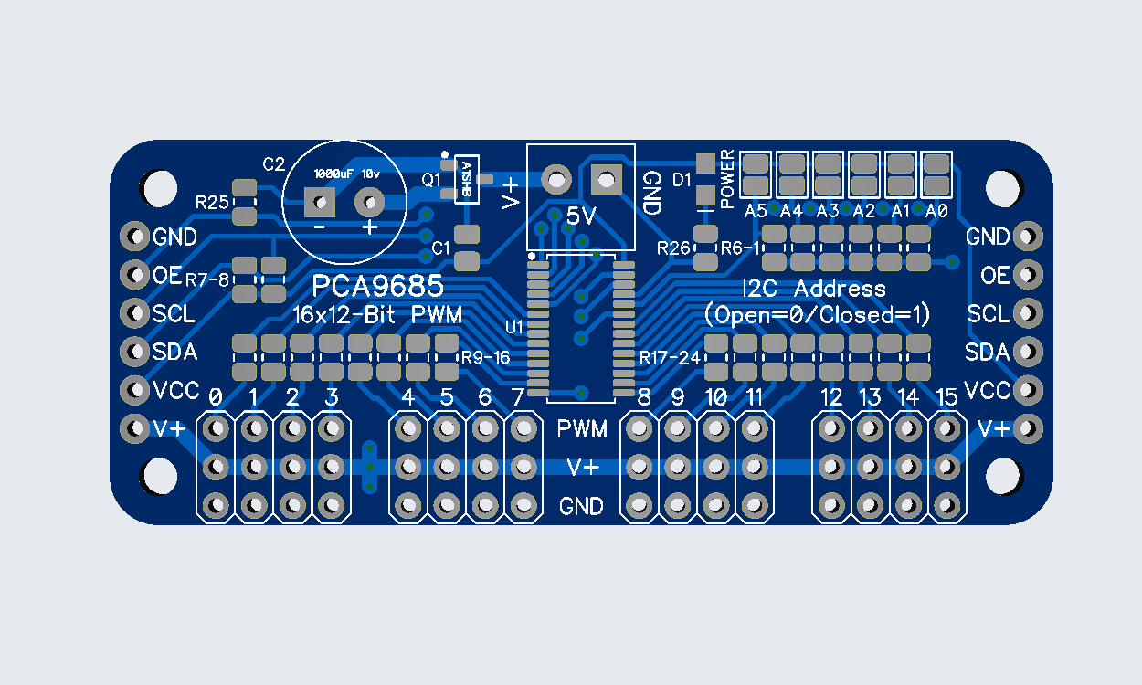
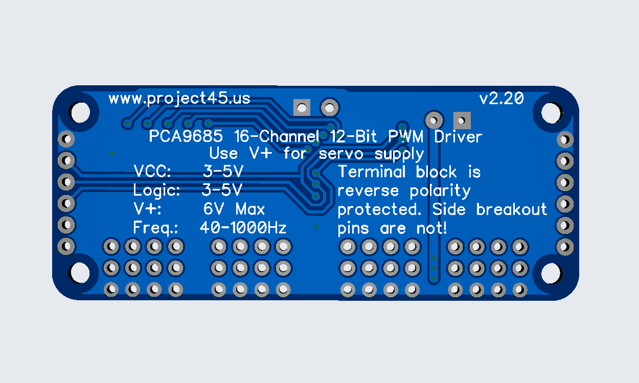
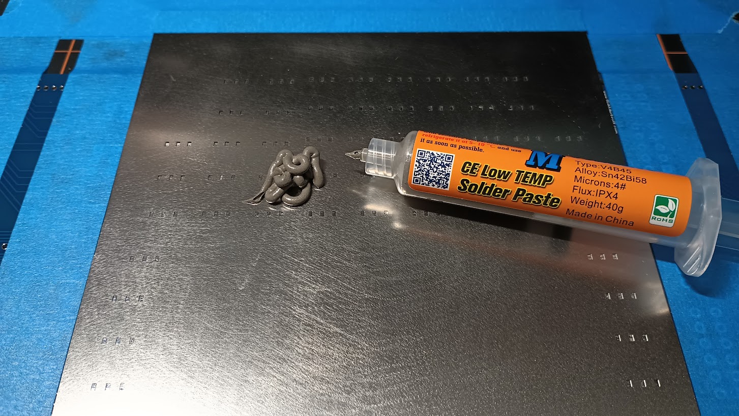
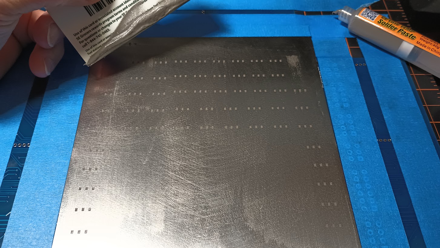
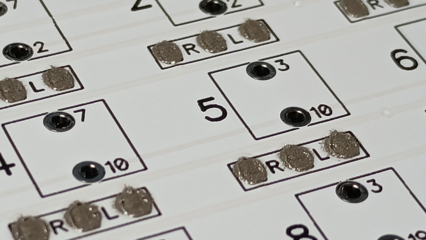
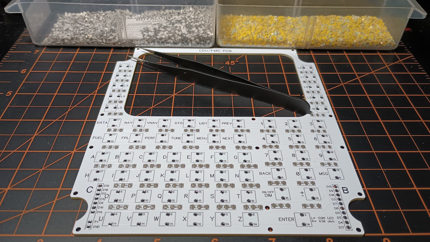
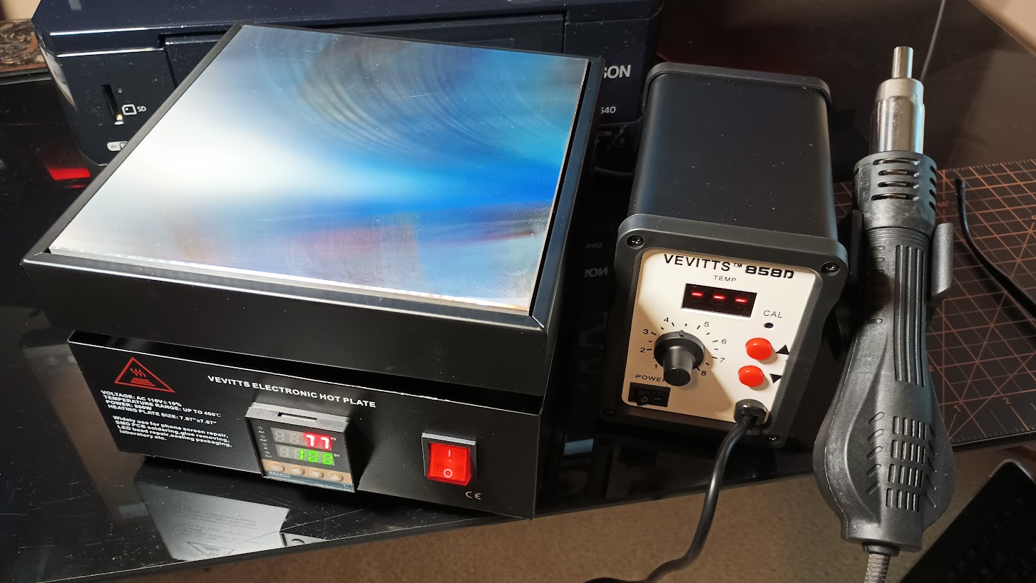
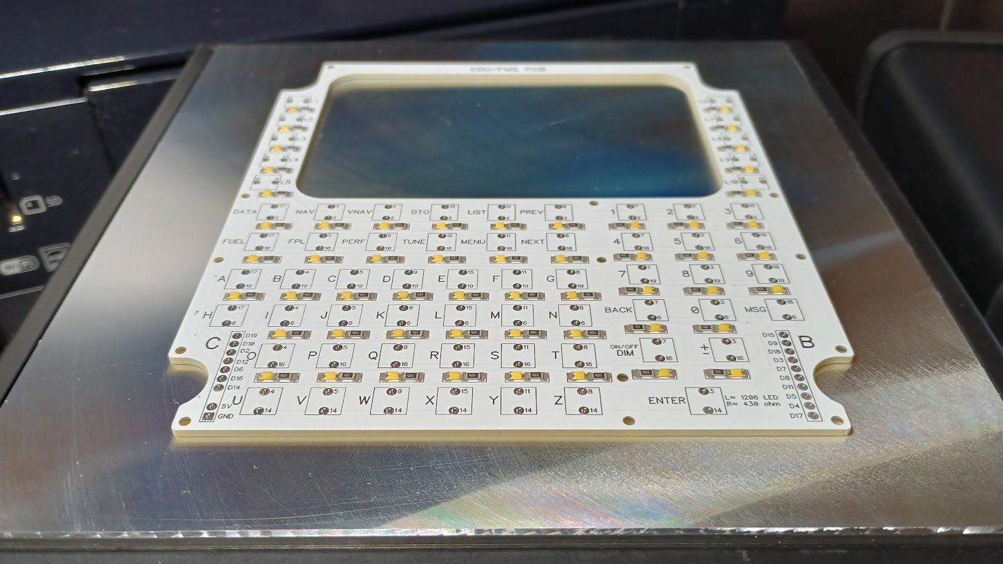
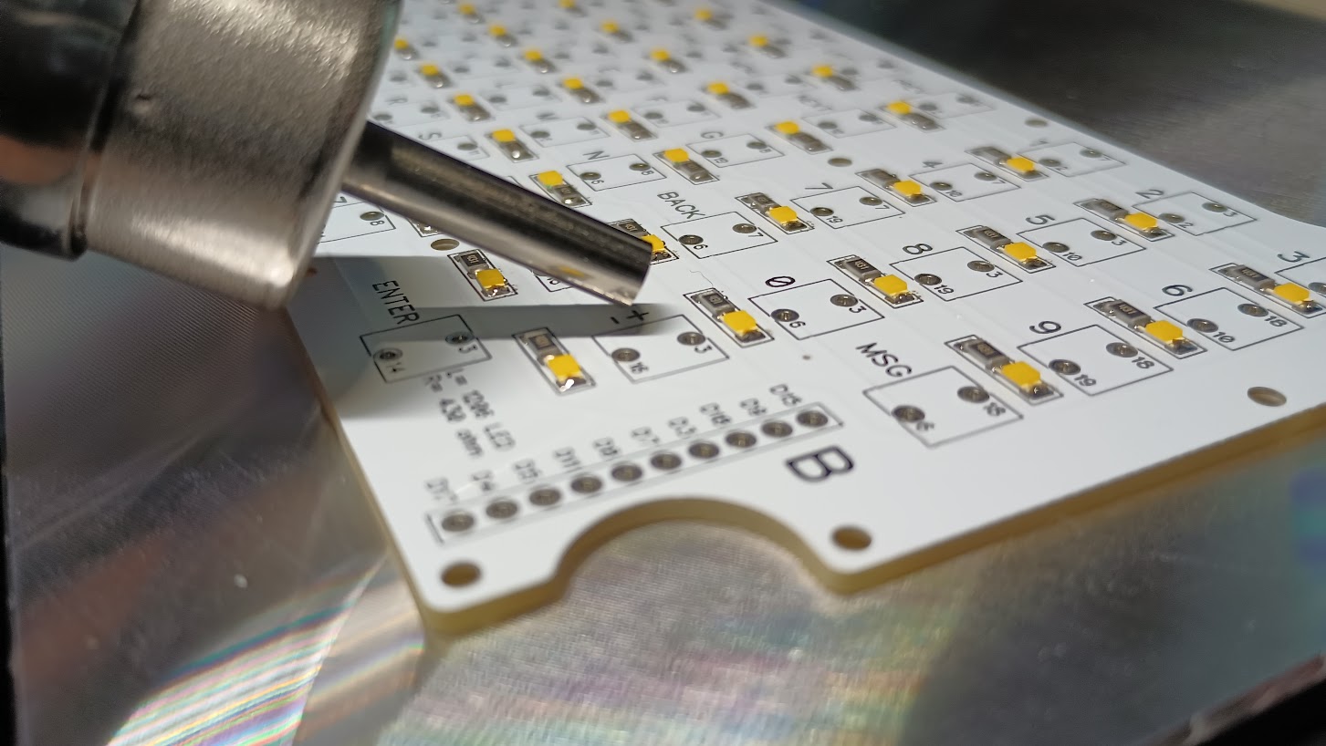
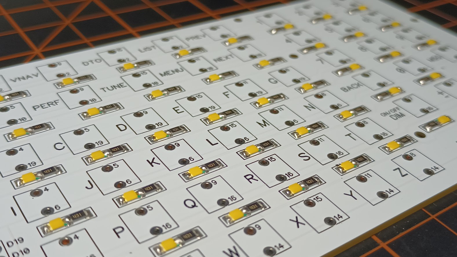
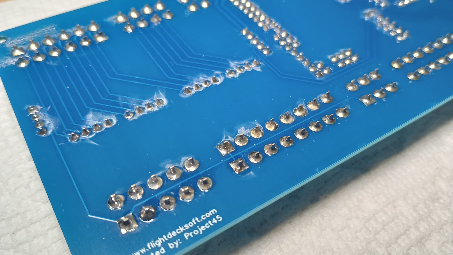
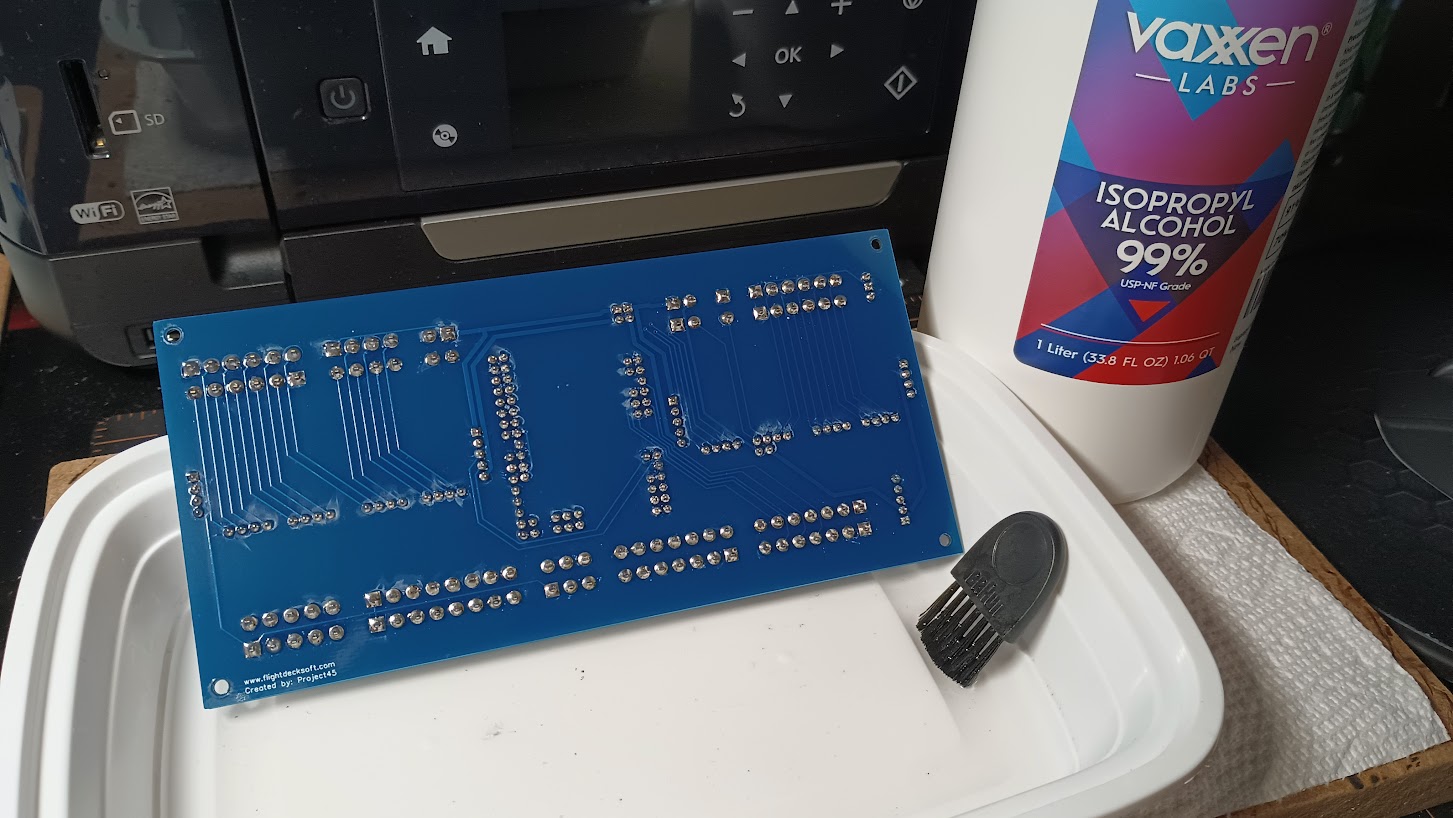
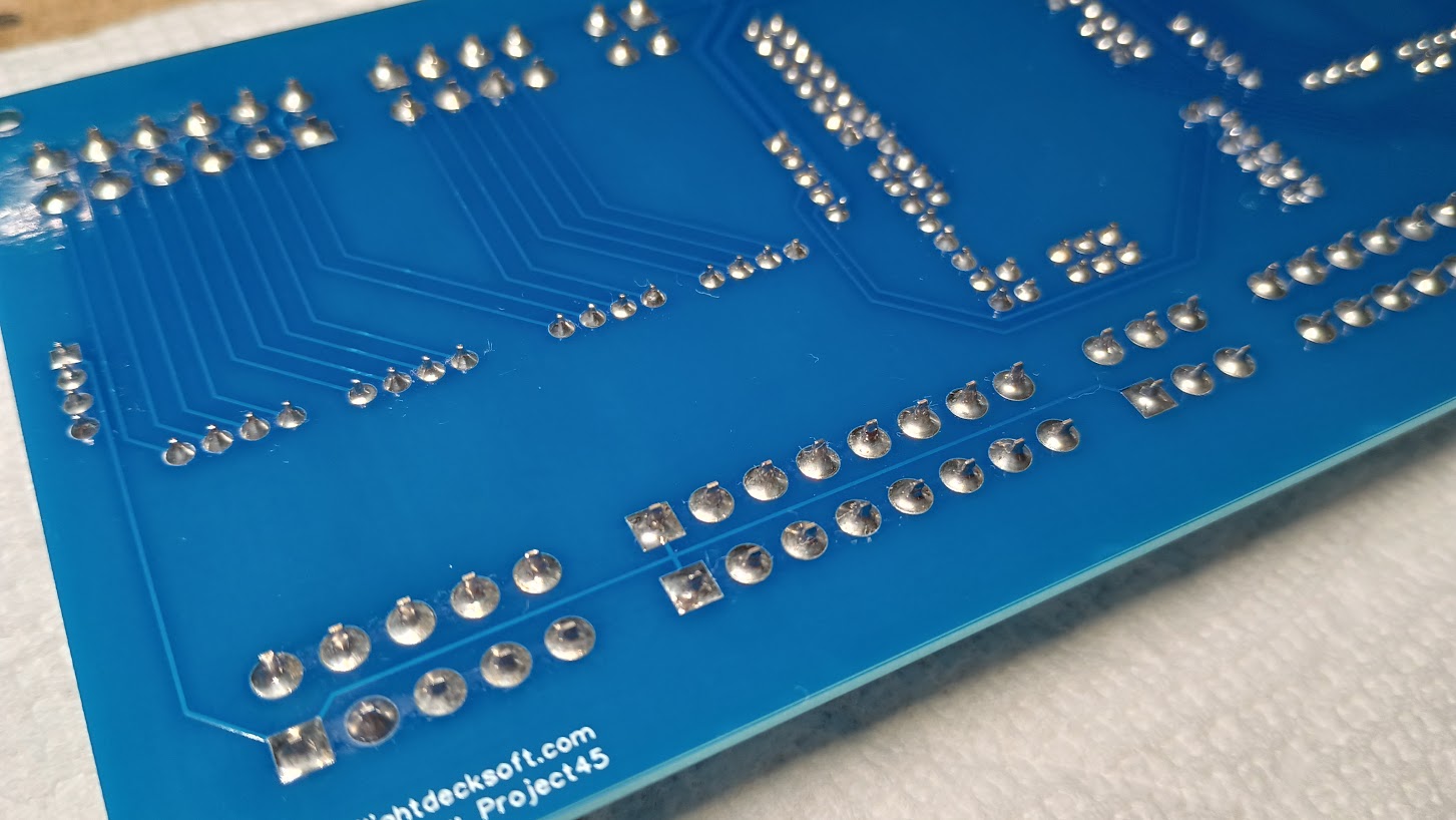
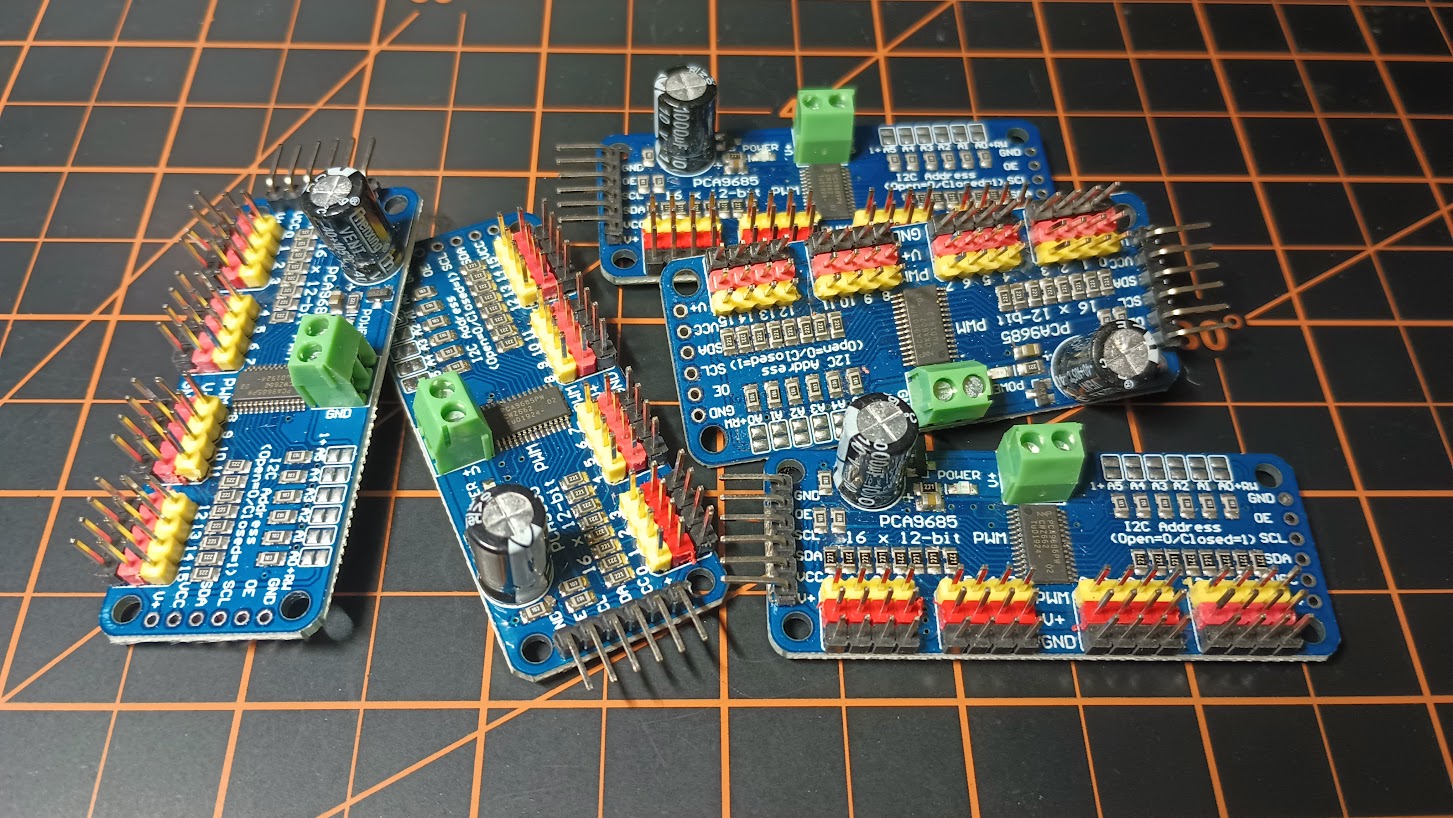
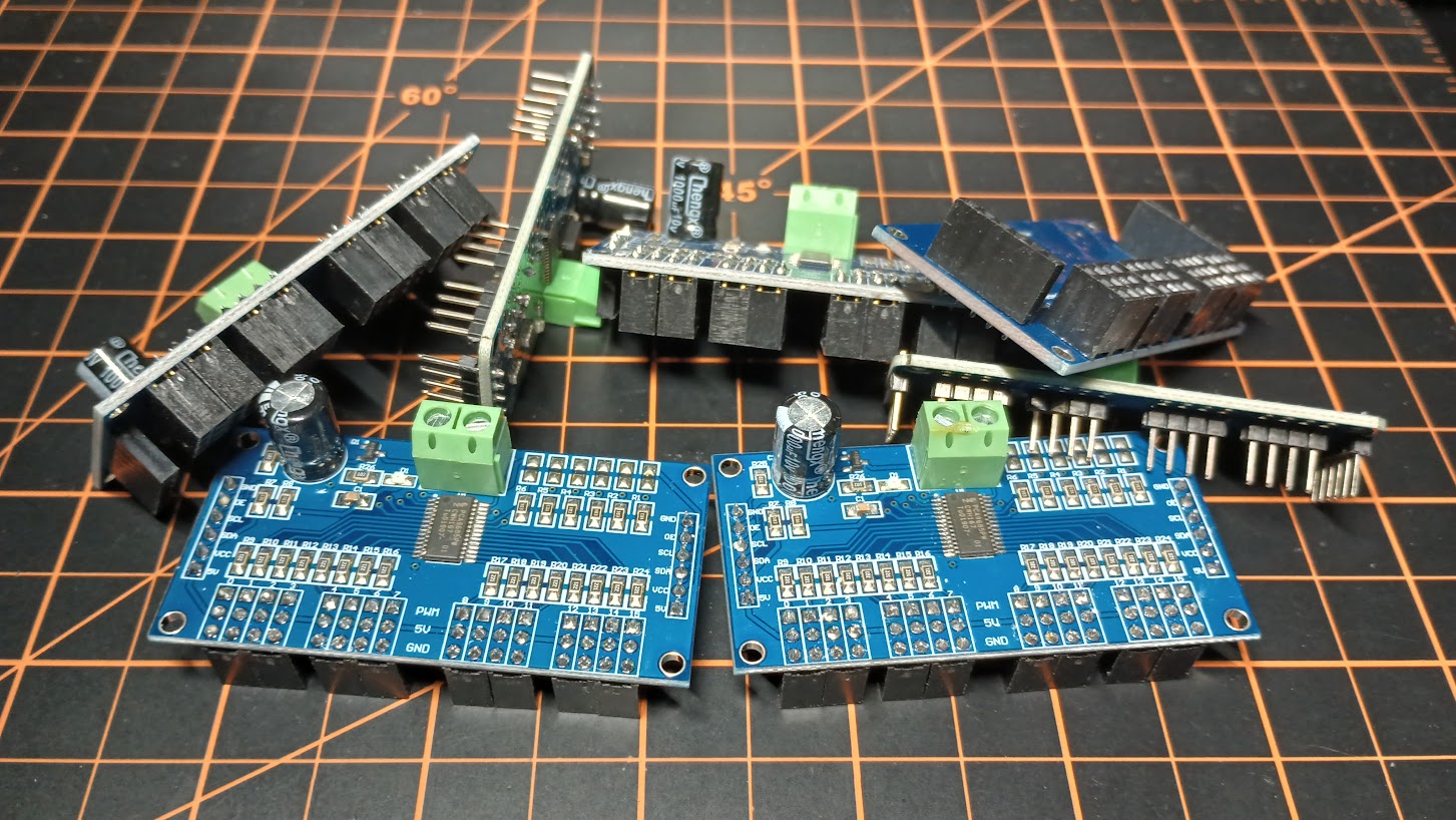
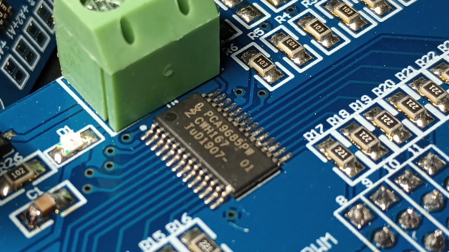
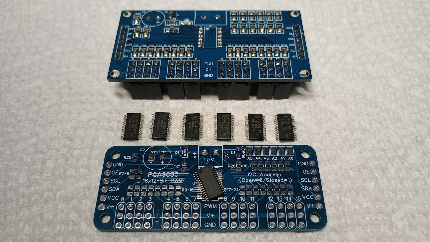
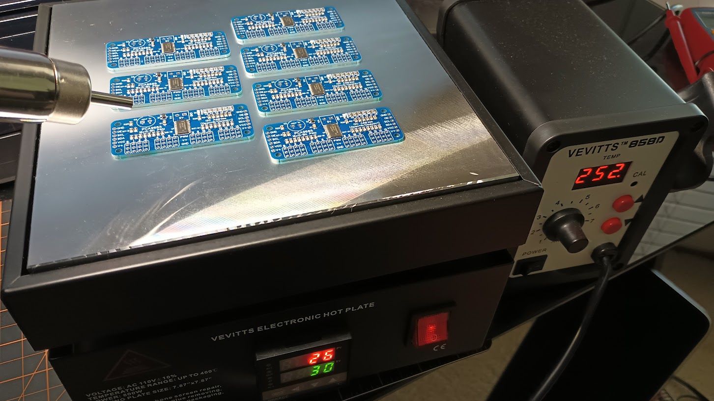
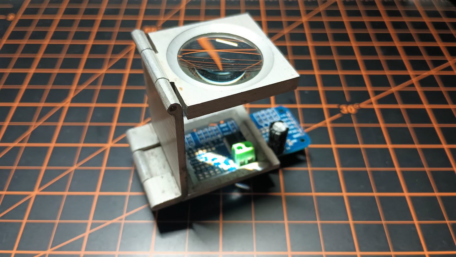
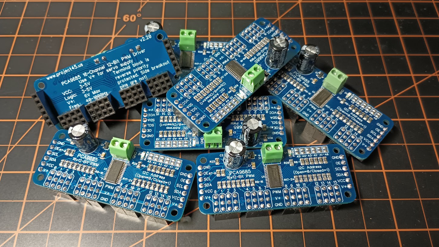
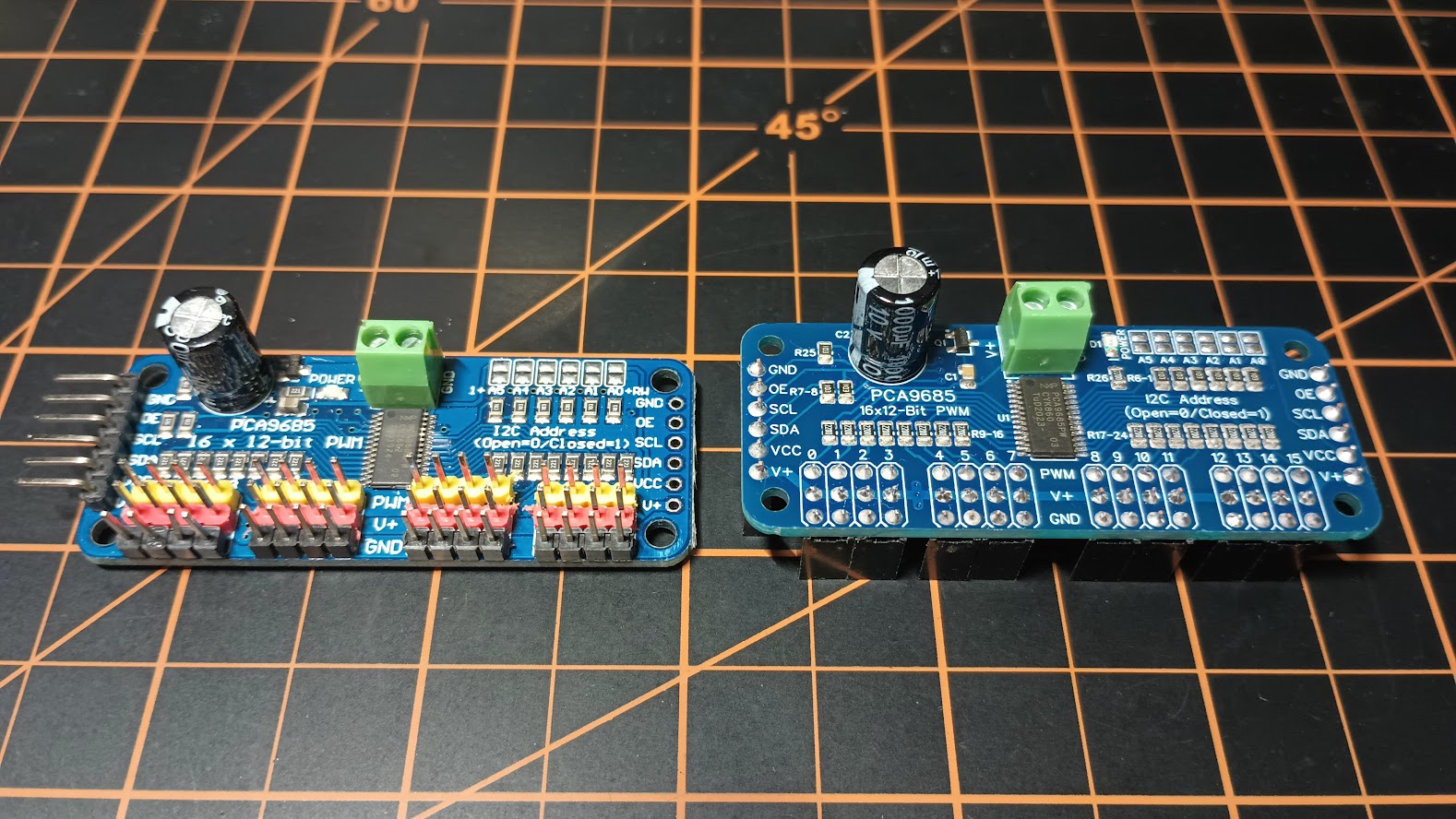
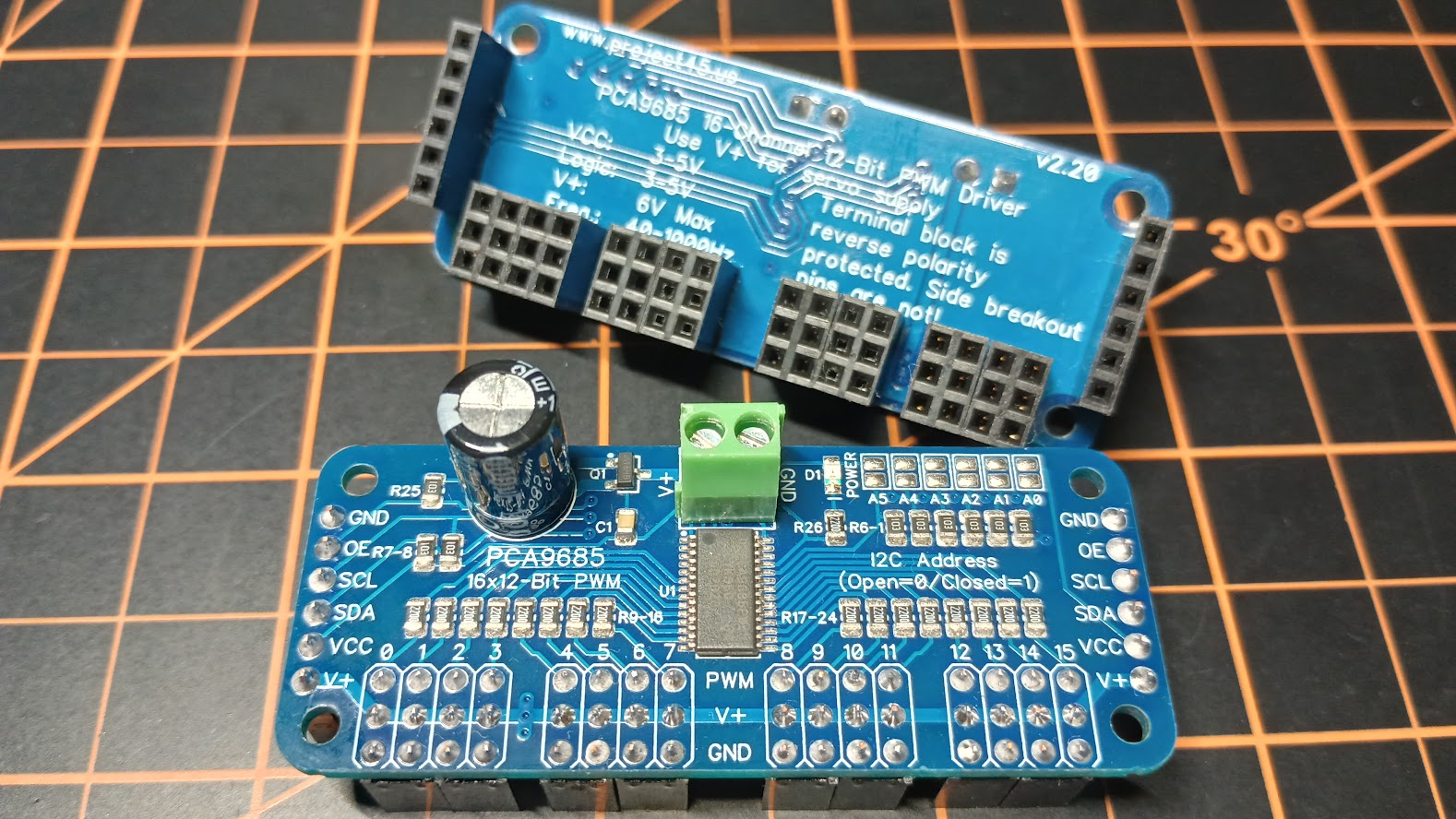
Hey guys, First I have to thank Jason for encouraging me to move forward on developing our own pcb modules a few years back. This is one of those areas where looking back now, I wonder how we did without. And thanks to Will for helping out with pointing me to JLCPCB, a pcb prototyping/manufacturing company that makes it very easy and affordable to make parts. Recently Jason and I were discussing the availability of the 16 Channel PWM LED Drivers. Although there are a dozen options out there, the ones we prefer to make things easy for us are getting harder to find at a decent price. It got me to thinking why not make our own so that we have some control over availability, cost, what pin blocks are soldered to them and color. One fear of designing a sim as en depth and complicated as what we are doing here is parts going obsolete with time. I believe the 16 Channel PWM will be here for the next 25 plus years in one form or another but there are other parts and modules that may not have such a long availability span, such as the compact Meduino Mega2560 Pro Mini, a knock off of the Arduino260. To date, I believe there is only one manufacturer of this board and they are already getting hard to find. Here is an authentic Arduino 2560 in comparison. In our case, the Meduino 2560 Pro Mini is the perfect size and fit for our Interface modules with the pin headers mounted to the rear of the board. (In the case of the Meduino above, there are no headers mounted to the board yet). The Meduino works exactly the same as the original Arduino and any software running through it would not know the difference. My hopes are that several companies pick up on the Meduino and flood the market with knockoffs so that we never have to worry about availability. But just in case this does not happen, I want to get ahead of the curve and start developing my own pcb design skills to take on the Meduino 2560 myself. And now you know the back story of why I am interested in "redesigning the wheel"! In order to get to the point where I am able to develop a knock off version of the 2560 Pro Mini, I first had to take on something not as complicated. And that brings us back to the 16 Channel PWM. As I mentioned before, there are dozens of options out there but none of them match our exact needs, although they all operate exactly the same. Here are several examples. The example in the top right corner is what we need, female headers soldered to the back side of the board. The most common 16 Channel PWM is the one with the multi color male headers soldered to the top of the board. If you are lucky, you will find boards like the two examples at the bottom or the purple one with no headers soldered to them where we can add them ourselves. Several weeks back I started working on the design process of our very own 16 Channel PWM. Between having limited information on the fine details and having a couple good examples on hand, I was able to reverse engineer the PWM. And this is what it looks like! It will operate the same as all the other PWMs and is the same size as a standard PWM, although I have found that not all PWMs have the same pin footprint. I used AutoSketch9 to first draw the PWM and then DipTrace to create the pcb and the Gerber file needed by the manufacturer. As I mentioned above, I use a company called JLCPCB to do the manufacturing. PCBWay is also a great company to have your prototype PCB made at a low cost. Currently I have 100 pieces ordered including a stencil so that I can easily apply solder paste to the pads to make the soldering process of the SMDs as easy as possible. The order should arrive in about eight days. During this PWM PCB project, I picked up several new skills I had not yet used in all the previous PCB projects. The PWM is a little more complicated than the interface breakout boards and required me to "step up" my skills and knowledge base. The biggest challenge in my mind was worrying about soldering the PCA9685 chip to the board. My soldering skills are good but there is no way to solder super small legs to super small SMD pads using a soldering iron! I was all set up to have the manufacturer assemble the SMD components (at a cost), but after watching a ton of YouTube videos, I decided to use a hotplate and a hot airgun to do the job. (This is similar to the way Will does his SMD soldering.) I learned a couple new terms like "solder reflow" and "surface tension". The hardest part will be to get the solder past onto the pcb exactly where the pads are, but that is not that big of a deal for a couple reasons. First, when I placed the order with JLCPCB, I also ordered the stencil for the PWM. At only $7, it will be well worth the cost. Here is an example of a solder paste stencil making the process easy. https://youtu.be/SPzvIXPq4QY The second reason why applying solder paste onto the PCB is not a big deal is because the reflow process is very forgiving. If you add to much, it can be removed after the reflow process. If your parts start off a little crooked, the reflow process will straighten them up via surface tension, also known as magic. Another short video. https://youtu.be/sZpY5RL6jw8 Once, I get the pcb and stencil in hand, I will update this thread with my own photos and videos. Another area that I have not had to work with until the PWM project was placing copper pours. This is the first time that I have had to use a copper pour. If you are not familiar with what it is, take a look at the two PWM drawing photos above. The back side of the PWM has a copper pour in place. Most all pcb has either one or both sides of the board copper poured. Basically, you can use the copper pour area as a signal or net. In the case above, I am using the copper pour as the ground. It can reduce the amount of trace lines and vias. (Vias are holes connecting the front side of the board to the rear, or multiple layers within, which in the case of the PWM, it only has two layers). Speaking of vias, I found it interesting that I was able to design my version of the PWM using only 21 vias. The other examples have no less than 25 and as many as 28 vias. I think the reason for this is because of the auto route function in DipTrace. DipTrace and other PCB programs have the ability to automatically route all the ratlines at once. A ratline is a straight line connection between two or more pins or pads. They call them ratlines because before they are routed, all the ratlines together look like a rat's nest! What I have found is that using the auto route function will get you close, but it is far from perfect. If you want perfect or as close to perfect as possible, you have to manually route your ratlines. In smaller projects, like the PWM, manual routing is possible, but in larger projects, you first have to select auto route to create a starting point. Then you can modify the trace lines manually. Based on what I have seen in these PWM examples I have been studying, whoever did the trace lines used the auto route function with very little manual modifications. Just an observation. I have picked up a ton of other knowledge and skills based on this PWM project which will help prepare me for the larger 2560 Pro Mini design. I will have another update once the PWM PCB order arrives! Hey guys, First I have to thank Jason for encouraging me to move forward on developing our own pcb modules a few years back. This is one of those areas where looking back now, I wonder how we did without. And thanks to Will for helping out with pointing me to JLCPCB, a pcb prototyping/manufacturing company that makes it very easy and affordable to make parts. Recently Jason and I were discussing the availability of the 16 Channel PWM LED Drivers. Although there are a dozen options out there, the ones we prefer to make things easy for us are getting harder to find at a decent price. It got me to thinking why not make our own so that we have some control over availability, cost, what pin blocks are soldered to them and color. One fear of designing a sim as en depth and complicated as what we are doing here is parts going obsolete with time. I believe the 16 Channel PWM will be here for the next 25 plus years in one form or another but there are other parts and modules that may not have such a long availability span, such as the compact Meduino Mega2560 Pro Mini, a knock off of the Arduino260. To date, I believe there is only one manufacturer of this board and they are already getting hard to find. Here is an authentic Arduino 2560 in comparison. In our case, the Meduino 2560 Pro Mini is the perfect size and fit for our Interface modules with the pin headers mounted to the rear of the board. (In the case of the Meduino above, there are no headers mounted to the board yet). The Meduino works exactly the same as the original Arduino and any software running through it would not know the difference. My hopes are that several companies pick up on the Meduino and flood the market with knockoffs so that we never have to worry about availability. But just in case this does not happen, I want to get ahead of the curve and start developing my own pcb design skills to take on the Meduino 2560 myself. And now you know the back story of why I am interested in "redesigning the wheel"! In order to get to the point where I am able to develop a knock off version of the 2560 Pro Mini, I first had to take on something not as complicated. And that brings us back to the 16 Channel PWM. As I mentioned before, there are dozens of options out there but none of them match our exact needs, although they all operate exactly the same. Here are several examples. The example in the top right corner is what we need, female headers soldered to the back side of the board. The most common 16 Channel PWM is the one with the multi color male headers soldered to the top of the board. If you are lucky, you will find boards like the two examples at the bottom or the purple one with no headers soldered to them where we can add them ourselves. Several weeks back I started working on the design process of our very own 16 Channel PWM. Between having limited information on the fine details and having a couple good examples on hand, I was able to reverse engineer the PWM. And this is what it looks like! It will operate the same as all the other PWMs and is the same size as a standard PWM, although I have found that not all PWMs have the same pin footprint. I used AutoSketch9 to first draw the PWM and then DipTrace to create the pcb and the Gerber file needed by the manufacturer. As I mentioned above, I use a company called JLCPCB to do the manufacturing. PCBWay is also a great company to have your prototype PCB made at a low cost. Currently I have 100 pieces ordered including a stencil so that I can easily apply solder paste to the pads to make the soldering process of the SMDs as easy as possible. The order should arrive in about eight days. During this PWM PCB project, I picked up several new skills I had not yet used in all the previous PCB projects. The PWM is a little more complicated than the interface breakout boards and required me to "step up" my skills and knowledge base. The biggest challenge in my mind was worrying about soldering the PCA9685 chip to the board. My soldering skills are good but there is no way to solder super small legs to super small SMD pads using a soldering iron! I was all set up to have the manufacturer assemble the SMD components (at a cost), but after watching a ton of YouTube videos, I decided to use a hotplate and a hot airgun to do the job. (This is similar to the way Will does his SMD soldering.) I learned a couple new terms like "solder reflow" and "surface tension". The hardest part will be to get the solder past onto the pcb exactly where the pads are, but that is not that big of a deal for a couple reasons. First, when I placed the order with JLCPCB, I also ordered the stencil for the PWM. At only $7, it will be well worth the cost. Here is an example of a solder paste stencil making the process easy. The second reason why applying solder paste onto the PCB is not a big deal is because the reflow process is very forgiving. If you add to much, it can be removed after the reflow process. If your parts start off a little crooked, the reflow process will straighten them up via surface tension, also known as magic. Another short video. Once, I get the pcb and stencil in hand, I will update this thread with my own photos and videos. Another area that I have not had to work with until the PWM project was placing copper pours. This is the first time that I have had to use a copper pour. If you are not familiar with what it is, take a look at the two PWM drawing photos above. The back side of the PWM has a copper pour in place. Most all pcb has either one or both sides of the board copper poured. Basically, you can use the copper pour area as a signal or net. In the case above, I am using the copper pour as the ground. It can reduce the amount of trace lines and vias. (Vias are holes connecting the front side of the board to the rear, or multiple layers within, which in the case of the PWM, it only has two layers). Speaking of vias, I found it interesting that I was able to design my version of the PWM using only 21 vias. The other examples have no less than 25 and as many as 28 vias. I think the reason for this is because of the auto route function in DipTrace. DipTrace and other PCB programs have the ability to automatically route all the ratlines at once. A ratline is a straight line connection between two or more pins or pads. They call them ratlines because before they are routed, all the ratlines together look like a rat's nest! What I have found is that using the auto route function will get you close, but it is far from perfect. If you want perfect or as close to perfect as possible, you have to manually route your ratlines. In smaller projects, like the PWM, manual routing is possible, but in larger projects, you first have to select auto route to create a starting point. Then you can modify the trace lines manually. Based on what I have seen in these PWM examples I have been studying, whoever did the trace lines used the auto route function with very little manual modifications. Just an observation. I have picked up a ton of other knowledge and skills based on this PWM project which will help prepare me for the larger 2560 Pro Mini design. I will have another update once the PWM PCB order arrives! Hey guys, I have had a chance to play with the stencils, the hot plate and the hot air rework station. All pretty cool tools to help get the job(s) done! I think the stencils will come in very handy when it comes to jobs that have a ton of SMDs or pcb where the components are super tiny. Because I am in the process of building up several CDUs, I decided to use the CDU pcb stencil as an example in this post. Remember, the cost to have a metal stencil made is next to nothing with JLCPCB, just $6 and I would imagine that other major pcb manufacturers would have similar prices. There are a couple keys to using a stencil. First, you have to make sure the stencil is perfectly lined up on top of your pcb piece(s). I say pieces because if you choose to, you can have a stencil made that will do several pieces at a time. Second key, use decent solder paste. Without buying or making a fancy contraption, most guys in our situation would do something along the lines of what I did below. Here I am using unused FGC pcb to boarder the left, top and right sides of the CDU pcb. The CDU pcb stencil is taped across the top and is hinged in place so that when it is laid down, the holes in the stencil line up perfectly with the solder pads on the pcb. I finally found a suitable use for my SE Grocers Rewards card! It will be used to spread the solder pasted around and into the tiny pockets in the stencil. I am pretty sure your sorry unused rewards card will work too. I used Mechanic CE Low Temp Solder Paste. It has a melting point at 138c which is lower than usual. Using low melting point solder only becomes an issue if the components you are soldering get hot enough to approach this temp. In our case, we have nothing to worry about with our project pcbs....so far. These solder paste tubes come with tiny pin point applicators if you are doing isolated repairs. I also just read on the tube, "Solder paste is a high-end product with sensitive temperature. Please refrigerate at 5-10c and use as soon as possible." I wish I had read that first before buying a couple tubes of it that I will not need anytime soon and storing it in the upstairs bonus room in the Florida heat! With that said, the solder paste still appears to be performing well. However, I think excessive heat and time will wreck it. Lesson learned. Only buy one tube at a time and stick it in the frig next to the ketchup! As long as your stencil is lined up with your pcb and it is secure, spreading the solder paste around in the tiny openings was almost too easy! Go Rewards card! Turns out that the small amount I squeezed on the stencil was enough to do seven CDUs. That's over 1,100 smd pads! Time wise after getting set up, I was able to apply solder paste to all the CDU pcbs in less than 5 minutes. I could have done it much faster but being it was my first time, I wanted to make sure I was doing it right. What you end up with is just the right amount of solder paste on each of the smd pads. The solder paste is very forgiving. If you end up putting too much on or everywhere, it wipes up nicely. Or, if you are already at the "heating up" stage, the solder paste gets drawn to the smd pad. (See video in previous post) Now the time consuming part but not bad. Unless you are paying for SMT (Surface Mount Technology), in other words, having the pcb manufacturer assemble the SMD components onto your pcb, there is no getting around this step. Each SMD component has to be placed on it's solder pad and you have to make sure everything is oriented correctly. In the case of the CDU pcb, we are only dealing with resistors that can be placed in either direction and LEDs, which do have to be placed in one direction. Not a big deal, just takes a little time and paying attention. And this brings us to the next area of trying something new! Hot plates and Hot Air Rework Stations. I did my fair share of research on these tools and found unless you are looking for high end equipment, most of these things utilize the same exact design features, flaws and all! I figured I would start at the low end of the price spectrum. The Vevitts Hot plate for $71 HERE The Vevitts Hotair Rework Station for $39 HERE The only thing I think I will rework is add another power switch to the Hot Plate. Several folks who have this item and others like it add a second power switch that kills the power to the heating elements while maintaining power to the digital display so that you can observe the temperature coming back down. Otherwise, when you turn off the power switch, you are killing all the power to the Hot Plate including the digital display. (Rainy day project) Here I have all the LEDs and resistors sitting in position on top of tiny pockets of solder paste. One cool thing about the solder paste is it's sticky enough to hold components like these in place without fear of them sliding around. But still super easy to maneuver them or line them up. I have to say that this post is not meant to be a full blown tutorial on hot plate and hot air soldering. I would suggest watching a couple YouTube videos on the subject if you are not familiar with it. With that said, the main idea is to provide heat to the pcb from both sides. The hot plate from the bottom side and hot air from the top. What is really cool about both the hot plate and the hot air rework station is you can dial in the exact temperature. As an example, the solder paste I am using has a melting temp of 138C. If I dial in 138C, you might see some solder paste starting to melt. But dial up another 5C over (143C) and more solder paste begins to melt. Dial in 10C over (148C) and most all the solder paste melts. And that is where the hot air rework station comes in. I had the hot air set at 150C and in areas where the hot plate needed backup, the hot air is enough to push it over the top. This method keeps you from having to dial up 185C on the hot plate to insure everything gets melted. At some point, there is a such thing as too much heat and the pcb will start to become damaged. I have not seen it myself so far, but I have seen others in videos burn, melt and warp their pcbs. The goal is to get everything melted as quickly as possible at the lowest temperature possible without over exposing our pcb to too much heat. As soon as I pulled the pcb off of the hot plate and let it cool down, I did a light test. PASS Now with everything confirmed working and in place, I took a few minutes to add a little solder the old fashion way, using a soldering tip where it looked like it could use some extra. And that is pretty much it on stencils, hot plates and hot air rework stations. Great tools to help get us to our goals a little faster. I still have to manually solder in the through hole components like the buttons, but again, no big deal. One last thing about pcb. While gearing myself up to work with hot plates, etc, I ran across a couple videos of guys cleaning their pcbs. This is something that I have not done but will be starting now. If you have any of my pcb or you just have pcb that needs cleaning, check this out. I am using one of the large blue Panels Module pcbs because it shows the gunk better than the white pcb. As you can see, it does not look bad, but it can look better! Get yourself a 1 liter bottle of Vaxxen Isopropyl Alcohol 99%, a tiny brush and a small plastic tub. Most pcb components, like the good doc here don't mind an alcohol bath! https://hangar45.net/wp-content/uploads/2023/05/E75ShFG.mp4 (I might have the good doc do a tutorial for us in the future) Just be careful of sensitive sensors, like poteniometers as an example, if the board you are cleaning has them. Just scrub and rinse the board two or three times, wipe clean with a cotton cloth and that's it! Clean as a whistle. From here forward, I will be sending out all pcb "cleaned". Looks much better and professional. If anyone has any pcb tips, please share. I am no expert on any of this, remember, it was just a few weeks ago that all this was new to me as well. Hey guys, I have had a chance to play with the stencils, the hot plate and the hot air rework station. All pretty cool tools to help get the job(s) done! I think the stencils will come in very handy when it comes to jobs that have a ton of SMDs or pcb where the components are super tiny. Because I am in the process of building up several CDUs, I decided to use the CDU pcb stencil as an example in this post. Remember, the cost to have a metal stencil made is next to nothing with JLCPCB, just $6 and I would imagine that other major pcb manufacturers would have similar prices. There are a couple keys to using a stencil. First, you have to make sure the stencil is perfectly lined up on top of your pcb piece(s). I say pieces because if you choose to, you can have a stencil made that will do several pieces at a time. Second key, use decent solder paste. Without buying or making a fancy contraption, most guys in our situation would do something along the lines of what I did below. Here I am using unused FGC pcb to boarder the left, top and right sides of the CDU pcb. The CDU pcb stencil is taped across the top and is hinged in place so that when it is laid down, the holes in the stencil line up perfectly with the solder pads on the pcb. I finally found a suitable use for my SE Grocers Rewards card! It will be used to spread the solder pasted around and into the tiny pockets in the stencil. I am pretty sure your sorry unused rewards card will work too. I used Mechanic CE Low Temp Solder Paste. It has a melting point at 138c which is lower than usual. Using low melting point solder only becomes an issue if the components you are soldering get hot enough to approach this temp. In our case, we have nothing to worry about with our project pcbs....so far. These solder paste tubes come with tiny pin point applicators if you are doing isolated repairs. I also just read on the tube, "Solder paste is a high-end product with sensitive temperature. Please refrigerate at 5-10c and use as soon as possible." I wish I had read that first before buying a couple tubes of it that I will not need anytime soon and storing it in the upstairs bonus room in the Florida heat! With that said, the solder paste still appears to be performing well. However, I think excessive heat and time will wreck it. Lesson learned. Only buy one tube at a time and stick it in the frig next to the ketchup! As long as your stencil is lined up with your pcb and it is secure, spreading the solder paste around in the tiny openings was almost too easy! Go Rewards card! Turns out that the small amount I squeezed on the stencil was enough to do seven CDUs. That's over 1,100 smd pads! Time wise after getting set up, I was able to apply solder paste to all the CDU pcbs in less than 5 minutes. I could have done it much faster but being it was my first time, I wanted to make sure I was doing it right. What you end up with is just the right amount of solder paste on each of the smd pads. The solder paste is very forgiving. If you end up putting too much on or everywhere, it wipes up nicely. Or, if you are already at the "heating up" stage, the solder paste gets drawn to the smd pad. (See video in previous post) Now the time consuming part but not bad. Unless you are paying for SMT (Surface Mount Technology), in other words, having the pcb manufacturer assemble the SMD components onto your pcb, there is no getting around this step. Each SMD component has to be placed on it's solder pad and you have to make sure everything is oriented correctly. In the case of the CDU pcb, we are only dealing with resistors that can be placed in either direction and LEDs, which do have to be placed in one direction. Not a big deal, just takes a little time and paying attention. And this brings us to the next area of trying something new! Hot plates and Hot Air Rework Stations. I did my fair share of research on these tools and found unless you are looking for high end equipment, most of these things utilize the same exact design features, flaws and all! I figured I would start at the low end of the price spectrum. The Vevitts Hot plate for $71 HERE The Vevitts Hotair Rework Station for $39 HERE The only thing I think I will rework is add another power switch to the Hot Plate. Several folks who have this item and others like it add a second power switch that kills the power to the heating elements while maintaining power to the digital display so that you can observe the temperature coming back down. Otherwise, when you turn off the power switch, you are killing all the power to the Hot Plate including the digital display. (Rainy day project) Here I have all the LEDs and resistors sitting in position on top of tiny pockets of solder paste. One cool thing about the solder paste is it's sticky enough to hold components like these in place without fear of them sliding around. But still super easy to maneuver them or line them up. I have to say that this post is not meant to be a full blown tutorial on hot plate and hot air soldering. I would suggest watching a couple YouTube videos on the subject if you are not familiar with it. With that said, the main idea is to provide heat to the pcb from both sides. The hot plate from the bottom side and hot air from the top. What is really cool about both the hot plate and the hot air rework station is you can dial in the exact temperature. As an example, the solder paste I am using has a melting temp of 138C. If I dial in 138C, you might see some solder paste starting to melt. But dial up another 5C over (143C) and more solder paste begins to melt. Dial in 10C over (148C) and most all the solder paste melts. And that is where the hot air rework station comes in. I had the hot air set at 150C and in areas where the hot plate needed backup, the hot air is enough to push it over the top. This method keeps you from having to dial up 185C on the hot plate to insure everything gets melted. At some point, there is a such thing as too much heat and the pcb will start to become damaged. I have not seen it myself so far, but I have seen others in videos burn, melt and warp their pcbs. The goal is to get everything melted as quickly as possible at the lowest temperature possible without over exposing our pcb to too much heat. As soon as I pulled the pcb off of the hot plate and let it cool down, I did a light test. PASS Now with everything confirmed working and in place, I took a few minutes to add a little solder the old fashion way, using a soldering tip where it looked like it could use some extra. And that is pretty much it on stencils, hot plates and hot air rework stations. Great tools to help get us to our goals a little faster. I still have to manually solder in the through hole components like the buttons, but again, no big deal. One last thing about pcb. While gearing myself up to work with hot plates, etc, I ran across a couple videos of guys cleaning their pcbs. This is something that I have not done but will be starting now. If you have any of my pcb or you just have pcb that needs cleaning, check this out. I am using one of the large blue Panels Module pcbs because it shows the gunk better than the white pcb. As you can see, it does not look bad, but it can look better! Get yourself a 1 liter bottle of Vaxxen Isopropyl Alcohol 99%, a tiny brush and a small plastic tub. Most pcb components, like the good doc here don't mind an alcohol bath! (I might have the good doc do a tutorial for us in the future) Just be careful of sensitive sensors, like poteniometers as an example, if the board you are cleaning has them. Just scrub and rinse the board two or three times, wipe clean with a cotton cloth and that's it! Clean as a whistle. From here forward, I will be sending out all pcb "cleaned". Looks much better and professional. If anyone has any pcb tips, please share. I am no expert on any of this, remember, it was just a few weeks ago that all this was new to me as well. Hey guys, Several weeks ago I placed an order with my PCB manufacturing company and received 100 PCB PWM boards. I am just now getting around to working with them. To recap, Jason and I were concerned about the long term availability of the PWM boards and in the short term, the price of them going up. Additionally, finding them with none of the headers soldered in place was getting to be nearly impossible. The solution? Just make them ourselves! So today, I gathered up all the PWMs I had that would not fit onto our modules because of the wrong pin headers. Here are a couple examples of PWMs that will not work in our builds. You can find these all day long but the headers are on the wrong side of the board. Removing these headers without harming the board is possible, but very time consuming. I thought these PWMs would be a good idea but whoever made them stopped selling them about the same time they started selling them! Turns out that this was a good thing because we really needed to go with the "standard" size PWM which is about 20% smaller than these. But there is still some value in these unusable PWM boards. With the chip shortage over the past two years, the cost of what use to be a 50 cent PCA9685PW chip is now as much as $5 each. This is about the cost of the whole PWM board a couple years ago. I opted to remove the chips from the PWM boards with a soldering reheat gun and recycle them onto the new PWM boards I just had made. Here are some of the removed chips ready to be soldered to the new boards. Like with the CDU stencil in the previous post, I am using a PWM stencil here. The solder paste stencil saves so much time! With small quantity runs like this, a make shift stencil jig is all you need. A little solder paste and a maxed out credit card to spread the paste around and you are ready to drop the components on the boards. The cool thing about the heat plate is that you can do several smaller boards all at the same time. I used the soldering reheat gun to help things along here and there, but with enough time, I believe the heat plate will do the job all on it's own. Once the SMD components are in place, I had to solder the female headers that are on the rear of the board to the top side of the board. Last but not least, I soldered the 5v power header and the capacitor to the board. One thing I had to do was find my old magnifying loupe to take a SUPER close look at the pins on the chip to insure the soldering was good. I had to fix a few of them using copper braid to pull some of the solder out from between the pins. If my eyes weren't wrecked before, they are for sure now! Here I have several new PWMs ready to be tested with the recycled PCA9685PW chips. And here is a photo of a PWM on the left that we can not use in our build compared to the new one that we can use. They both operate exactly the same, it's just a matter of the type of headers they each have. A close up view of the new Project45 PWMs. If they work as good as they look, we are golden! Next step is testing them to make sure they work as designed. I spent a ton of time going over the design several times to insure I did not miss anything but until they are tested, we won't know. I will be sending several of these to Jason so he can put them through the ringer. Fingers crossed! If all goes well I will make these available to all of our Hnagr45 members. Hey guys, Several weeks ago I placed an order with my PCB manufacturing company and received 100 PCB PWM boards. I am just now getting around to working with them. To recap, Jason and I were concerned about the long term availability of the PWM boards and in the short term, the price of them going up. Additionally, finding them with none of the headers soldered in place was getting to be nearly impossible. The solution? Just make them ourselves! So today, I gathered up all the PWMs I had that would not fit onto our modules because of the wrong pin headers. Here are a couple examples of PWMs that will not work in our builds. You can find these all day long but the headers are on the wrong side of the board. Removing these headers without harming the board is possible, but very time consuming. I thought these PWMs would be a good idea but whoever made them stopped selling them about the same time they started selling them! Turns out that this was a good thing because we really needed to go with the "standard" size PWM which is about 20% smaller than these. But there is still some value in these unusable PWM boards. With the chip shortage over the past two years, the cost of what use to be a 50 cent PCA9685PW chip is now as much as $5 each. This is about the cost of the whole PWM board a couple years ago. I opted to remove the chips from the PWM boards with a soldering reheat gun and recycle them onto the new PWM boards I just had made. Here are some of the removed chips ready to be soldered to the new boards. Like with the CDU stencil in the previous post, I am using a PWM stencil here. The solder paste stencil saves so much time! With small quantity runs like this, a make shift stencil jig is all you need. A little solder paste and a maxed out credit card to spread the paste around and you are ready to drop the components on the boards. The cool thing about the heat plate is that you can do several smaller boards all at the same time. I used the soldering reheat gun to help things along here and there, but with enough time, I believe the heat plate will do the job all on it's own. Once the SMD components are in place, I had to solder the female headers that are on the rear of the board to the top side of the board. Last but not least, I soldered the 5v power header and the capacitor to the board. One thing I had to do was find my old magnifying loupe to take a SUPER close look at the pins on the chip to insure the soldering was good. I had to fix a few of them using copper braid to pull some of the solder out from between the pins. If my eyes weren't wrecked before, they are for sure now! Here I have several new PWMs ready to be tested with the recycled PCA9685PW chips. And here is a photo of a PWM on the left that we can not use in our build compared to the new one that we can use. They both operate exactly the same, it's just a matter of the type of headers they each have. A close up view of the new Project45 PWMs. If they work as good as they look, we are golden! Next step is testing them to make sure they work as designed. I spent a ton of time going over the design several times to insure I did not miss anything but until they are tested, we won't know. I will be sending several of these to Jason so he can put them through the ringer. Fingers crossed! If all goes well I will make these available to all of our Hnagr45 members.Designing and building PCB
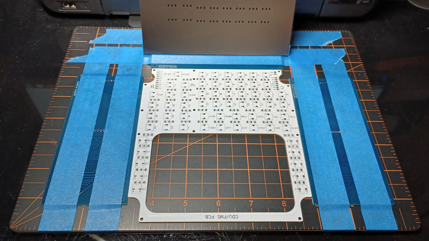
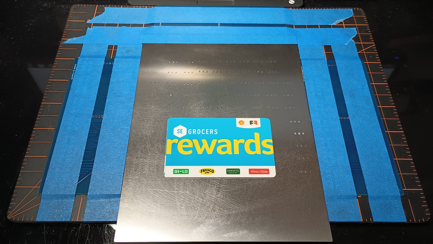
![]()
![]()
![]()
2017-10-10